The process of X-ray inspection method for PCBA and common welding defects
Source:H.F.XRelease time:2025-06-29 22:57:36
With the rapid development of new component packaging such as BGA and CPS packaging, the packaging volume of IC devices is becoming smaller and thinner, and the density of lead out terminals is increasing. The lead out terminals are also transferred from the periphery of the device to the bottom of the device. Nowadays, printed circuit board assemblies (PCBA) contain a large number of BGA, CPS packaging and other surface mount devices. Traditional detection technologies such as manual visual inspection and automatic optical inspection are almost powerless to detect the soldering quality of the bottom leads of such surface mount devices.

Principles of X-ray Testing
X-rays are electromagnetic waves with extremely short wavelengths and high energy, with strong penetration capabilities. When X-rays are irradiated on a sample, the transmission intensity is not only related to the energy of the X-rays, but also to the material density and thickness of the sample material. The smaller the material density and the thinner the thickness, the easier it is for X-rays to pass through.
The principle of X-ray detection is to use X-rays to irradiate the sample, and then use an image receiving and converting device to image the X-ray transmission intensity based on the contrast of grayscale brightness and darkness. PCBA contains a wide variety of materials with varying thicknesses, which are generally divided into four categories based on their material density:
Solder joints composed of tin, lead, or tin lead alloys with high material density;
Metal and ceramic packaging shells, gold wires, and chip bonding materials;
Plastic sealing materials, silicon and other easily permeable materials;
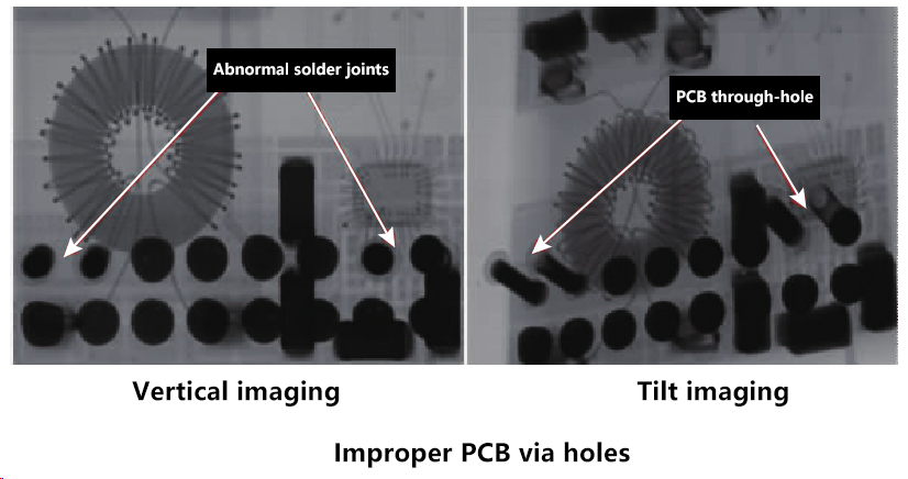
Defects such as voids, cracks, and PCB through holes.
When X-rays pass through the first and second types of materials, fewer X-rays pass through, resulting in higher grayscale values in the resulting image; When X-rays pass through the third category, the resulting image has a lower grayscale value; For the fourth category, X-rays completely penetrate and ultimately form bright images.

X-ray detection method
(1) Perform global inspection on PCBA, mainly including PCB and components;
(2) Enlarge the image for local inspection, search for defects or suspected defects;
(3) Identify, analyze, and confirm suspected defects through further magnification and oblique imaging;
(4) Perform oblique imaging on all BGA packaged devices to preliminarily check for virtual soldering defects. *Extended reading: X-Ray detection method for chip soldering bubbles

X-ray testing process
Usually, a PCBA contains several types of components, ranging from a few to dozens, with varying sizes and packaging. As a result, a PCBA may have multiple soldering defects simultaneously. Testing should not miss any type of defect while also considering efficiency, so engineering experience and a reasonable testing process are very important. Analyze the characteristics of various types of defects and identify specific types of defects in a targeted manner at each step of detection. The following is the X-ray inspection process for PCBA soldering quality, with each step having its own inspection purpose and focus.
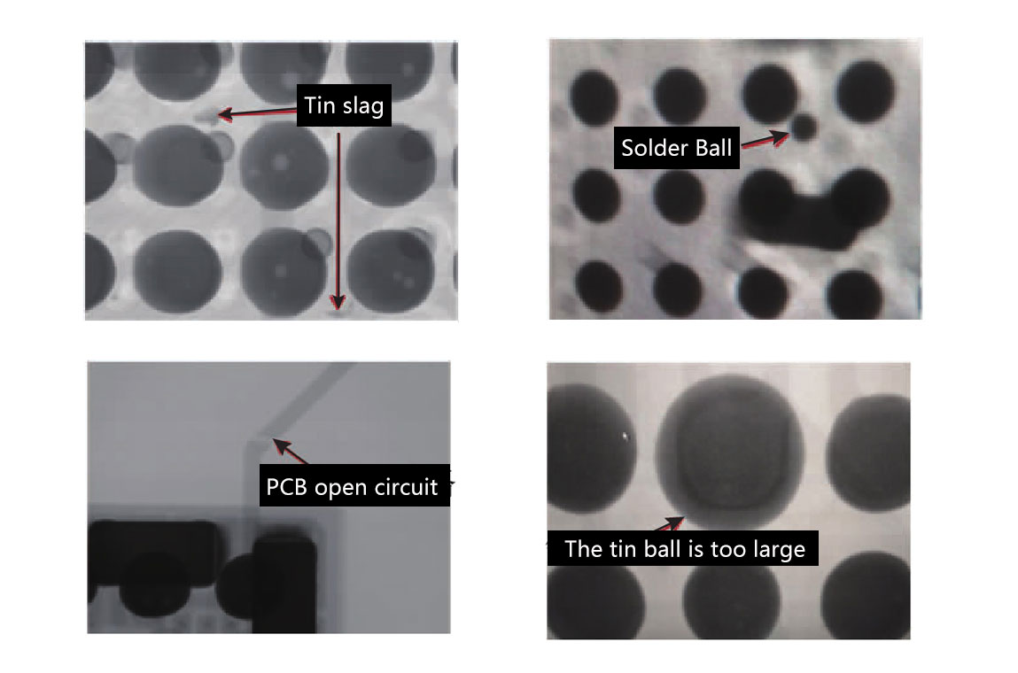
When conducting X-ray inspection, PCBA is generally divided into two main areas, namely the area covered by components and the area not covered by components. Defects such as PCB open circuit, solder slag, and solder beads can exist simultaneously in two areas, where solder slag and solder bead defects generally require oblique imaging to further confirm whether they are foreign impurities on the tray or carrier board.
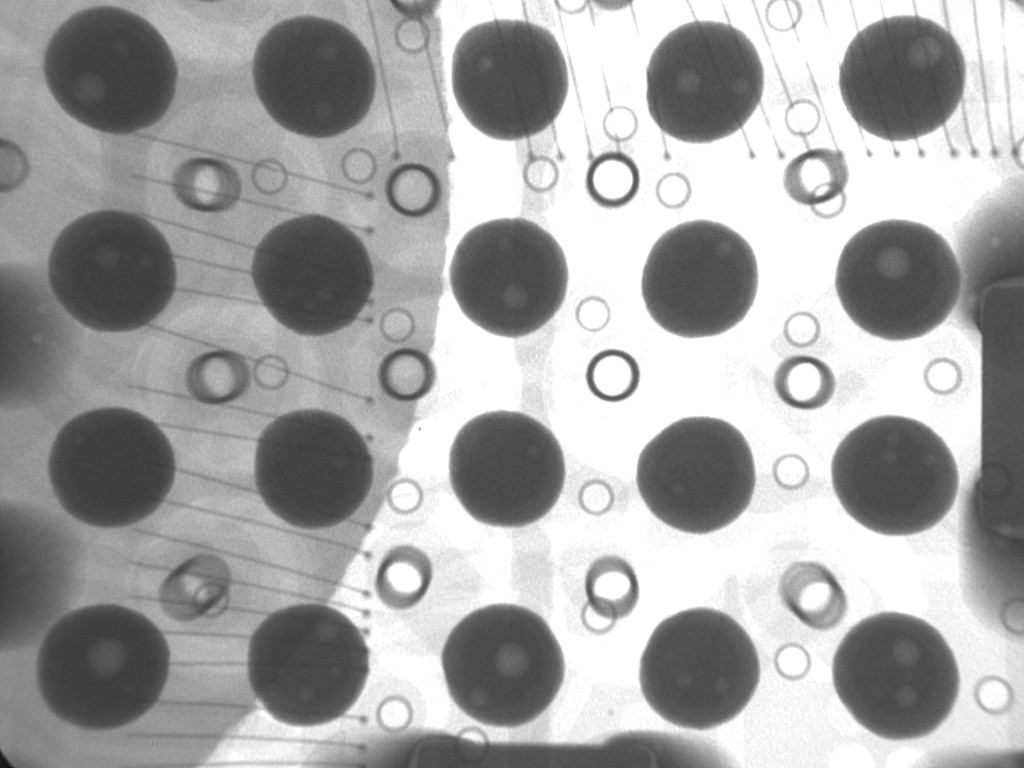
Hollow defects need to be further enlarged and confirmed, and measured. Currently, X-ray detection equipment generally integrates the calculation function of void area in the software. Voids that do not exceed the standard proportion in size are acceptable. The typical images of voids and void measurements are shown in the following figure.
Previous article:None
Next article:X-ray detection method for chip soldering bubbles
Recommend
-
The process of X-ray inspection method for PCBA and common welding defects
In the field of electronic manufacturing, product quality has always been the core of a company'
2025-06-30 -
The process of X-ray inspection method for PCBA and common welding defects
With the rapid development of electronic products towards miniaturization and high density, surface
2025-06-26 -
The process of X-ray inspection method for PCBA and common welding defects
Chip welding bubble detection technologyWith the miniaturization of integrated circuit devices and t
2025-06-26


