X-ray detection method for chip soldering bubbles
Source:H.F.XRelease time:2025-06-29 09:51:22
Chip welding bubble detection technology
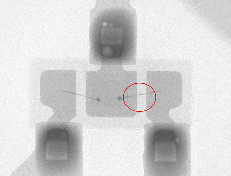
With the miniaturization of integrated circuit devices and the increasing demand for thermal reliability, the detection and control of chip soldering bubbles have become an important testing item to ensure the quality and reliability of chips. Chip soldering bubbles generally manifest as continuous large bubbles and randomly distributed small bubbles. These two types of bubbles have different effects on thermal resistance, but with the miniaturization of chips and the improvement of power density, the contribution of randomly distributed small bubbles to thermal resistance cannot be ignored.

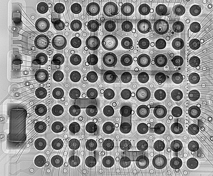
The non-destructive testing of chip soldering bubbles mainly includes two methods: micro focus X-ray (X-Ray) detection and acoustic scanning microscope (C-SAM). The scanning resolution of C-SAM can reach 0.1 μ m, and it has high sensitivity for bubble detection. The resolution of micro focus X-ray can also reach 0.1 μ m, which is suitable for detecting bubbles larger than 0.5mm, but it is more difficult to detect bubbles smaller than 0.5mm, especially when the background of the X-ray image is uneven, small bubbles are even more difficult to detect. However, C-SAM and X-Ray are complementary detection methods, and X-Ray has important practical application significance for bubble detection in SMT production process.

Recommend
-
X-ray detection method for chip soldering bubbles
In the field of electronic manufacturing, product quality has always been the core of a company'
2025-06-30 -
X-ray detection method for chip soldering bubbles
With the rapid development of electronic products towards miniaturization and high density, surface
2025-06-26 -
X-ray detection method for chip soldering bubbles
With the rapid development of new component packaging such as BGA and CPS packaging, the packaging v
2025-06-26


