Application of X-ray detection system for welding quality inspection of invisible solder joints in PCB assembly
Source:H.F.XRelease time:2025-06-29 09:20:30
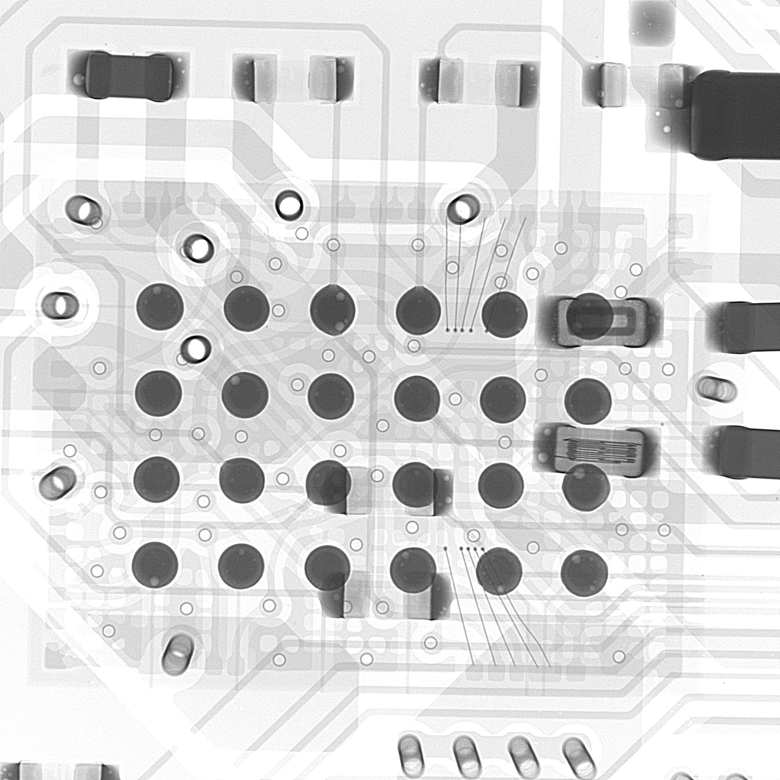
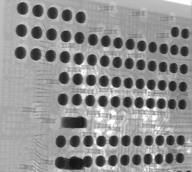
With the rapid development of electronic products towards miniaturization and high density, surface array devices such as BGA (ball grid array), FC (flip chip), and CSP (chip level packaging) are increasingly widely used in printed circuit board (PCB) assembly. One of the notable features of these devices is that their solder joints are often hidden beneath the packaging, making it difficult for traditional optical inspection methods to achieve. Therefore, in order to effectively ensure the welding quality of these invisible solder joints, X-ray inspection systems are playing an increasingly indispensable key role.

The core advantage of X-ray detection lies in its unique penetration ability. X-rays can penetrate packaging materials and directly image the shape and connection of internal solder joints, thereby determining the quality of their welding. In the face of the continuous trend of semiconductor component packaging technology evolving towards smaller sizes, when choosing an X-ray inspection system, it is necessary to fully consider the challenges of current and future component miniaturization on inspection accuracy.
High precision imaging and multi angle observation: core requirements for X-ray detection
To achieve accurate evaluation of the welding quality of invisible solder joints, the X-ray detection system must be able to provide high-definition
X-ray images. These images are the basis for analyzing potential welding defects such as open circuits, short circuits, virtual welding, bubbles, etc.
Therefore, the system must have sufficient magnification to meet the detection needs of smaller components both now and in the future. Only a
sufficiently detailed image can reveal the tiny abnormalities inside the solder joint.
In addition, for the analysis of solder joints in devices such as BGA and CSP, it is often not sufficient to observe them from a vertical perspective
(i.e., orthographic projection). Due to the three-dimensional structure of the solder ball, the information provided by a simple upward perspective
on the size, shape, and wetting condition of the solder ball may lack sufficient details, making it difficult to accurately determine the true state of
the welding. Therefore, advanced X-ray detection systems are usually equipped with tilt angle inspection function. By tilting the sample or X-ray
source/detector, solder joints can be observed from different angles to obtain more comprehensive three-dimensional information, thereby more
accurately evaluating the fullness of the solder joints, whether there are bridging or poor wetting issues, and so on.

Basic principles and types of X-ray detection systems
Fundamentally speaking, whether it is a two-dimensional (2D) or three-dimensional (3D) X-ray detection device, its basic principle is similar to
that of an X-ray projection microscope. The X-ray emission tube in the system generates an X-ray beam, which penetrates the sample being
tested (such as a PCB that has been welded). Due to the varying densities and atomic numbers of different materials (such as solder, copper,
substrate, etc.) in the sample, their absorption levels of X-rays also differ. The higher the density of a substance, the more it absorbs X-rays, and
the deeper the projection shadow it forms on the image receiver.
Geometric magnification is an important concept in X-ray imaging: the closer the tested sample is to the X-ray source, the larger the projected
image it forms on the detector, and vice versa. This principle enables the system to change the magnification of detection by adjusting the
distance between the sample and the radiation source.
In practical applications, there are multiple ways to implement X-ray detection systems:
*Two dimensional (2D) X-ray system
This is the most common type, which generates a two-dimensional planar image of the sample through a single X-ray projection. It can quickly
detect the basic condition of solder joints, such as bridging, solder ball loss, etc. 2D systems can be designed as online (integrated into the
production line for synchronous detection) or offline (independent of the production line for sampling or detailed analysis).
*Three dimensional (3D) X-ray system
In order to obtain more accurate internal structural information of solder joints, 3D X-ray technology has emerged. Recommended reading:
Comparison between 2D X-ray real-time detection system and 3D X-ray non-destructive testing technology, taking the effect of flip chip
devices as an example - Huafei (wahfei. cn)
*Computer tomography (CT) technology
Similar to medical CT scanning, this technology obtains two-dimensional projection images from multiple angles and uses complex
algorithms for reconstruction to generate clear images of a specific cross-section of the tested sample. This technology can provide very
detailed internal structural information, but due to the long time required for data acquisition and reconstruction (usually several minutes),
CT type X-ray systems are mainly used for offline professional research analysis and are not suitable for online detection that requires high
detection speed.
*X-ray Stratigraphy
This is another type of 3D X-ray detection technology. It reconstructs the image of the target cross-section by combining image data of
specific cross-sections and eliminating interference from other layers of image information. The X-ray layering system can also be designed
as online or offline, but in online applications, the detection speed is relatively slow due to the time required for image reconstruction.
For most production environments, whether it is 2D or 3D systems (except CT type), their design goal is to achieve the best image quality in
the shortest possible time, in order to reduce the cost of testing processes and improve production efficiency.
Recommend
-
Application of X-ray detection system for welding quality inspection of invisible solder joints in PCB assembly
In the field of electronic manufacturing, product quality has always been the core of a company'
2025-06-30 -
Application of X-ray detection system for welding quality inspection of invisible solder joints in PCB assembly
Chip welding bubble detection technologyWith the miniaturization of integrated circuit devices and t
2025-06-26 -
Application of X-ray detection system for welding quality inspection of invisible solder joints in PCB assembly
With the rapid development of new component packaging such as BGA and CPS packaging, the packaging v
2025-06-26


