


Application of X-ray inspection machine in electronic manufacturing such as PCB: void rate, solder filling, through-hole analysis, etc
Source:H.F.XRelease time:2025-07-06 17:04:27
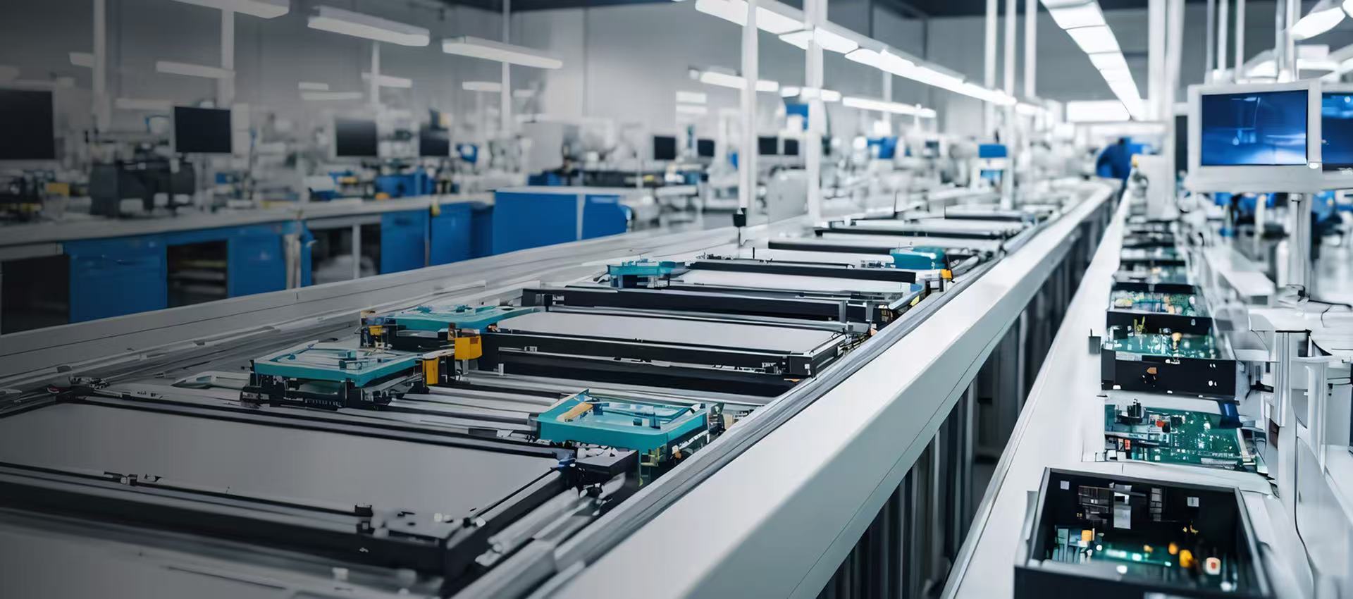
In the field of electronic manufacturing, product quality has always been the core of a company's competitiveness. Advanced X-ray detection
equipment is quietly changing everything. With advanced 2D and 3D inspection methods, this technology can capture tiny defects in printed
circuit boards and various electronic components in real time, ensuring that every product meets strict quality requirements.
High precision inspection is not only to identify obvious defects, but also to identify hidden dangers such as BGA voids, solder ball suction, and
component alignment deviations in advance. These issues are often difficult to detect in the early stages, but once overlooked, they may lead to
poor connections, short circuits, or even complete machine failure. Through precise data analysis, such as void ratio calculation and through-hole
filling detection, enterprises can grasp the internal condition of products at the early stage of production, take targeted improvement measures,
and reduce the risk of rework and repair.

【 ↑ Void calculation for void rate calculation 】
The advancement of technology has made the detection process more transparent and efficient. Advanced X-ray technology (H.F.X) can reconstruct clear 3D images from 2D slices, allowing engineers to intuitively observe the internal structure of components.

【 ↑ BGA Void Analysis void analysis 】
On the other hand, X-ray detection also demonstrates unparalleled advantages in addressing common issues such as insufficient solder filling. Through detailed scanning of the welding area, the detection system can quickly identify hidden dangers in through-hole welding, helping enterprises adjust the process in a timely manner and ensuring that every welding process can withstand the test. This precise detection not only maintains the functionality of the product, but also wins market reputation and user trust for the enterprise.

【 ↑ Solder Fill - X-ray inspection image of insufficient solder filling 】
In this series of testing processes, enterprises can use high-resolution 3D imaging technology to conduct detailed analysis of the through-hole area. Whether it is welding defects or small cracks, they can be captured in the first time. The application of this technology not only provides a guarantee for the stability of the product, but also provides data support for the subsequent technological improvement and quality enhancement of the enterprise.

【X-ray 3D Analysis of Through Hole Welding】
With these leading detection methods, electronic manufacturing enterprises can firmly occupy the forefront in the fiercely competitive market. Accurate data feedback and real-time quality monitoring provide scientific basis for each link, helping enterprises achieve continuous optimization in product development and production processes. For manufacturing enterprises that pursue high quality and reliability, adopting advanced X-ray inspection equipment is undoubtedly a wise way to reduce risks and save costs
Previous article:Application of X-ray detection system for welding quality inspection of invisible solder joints in PCB assembly
Next article:None
Recommend
-
Application of X-ray inspection machine in electronic manufacturing such as PCB: void rate, solder filling, through-hole analysis, etc
With the rapid development of electronic products towards miniaturization and high density, surface
2025-06-26 -
Application of X-ray inspection machine in electronic manufacturing such as PCB: void rate, solder filling, through-hole analysis, etc
Chip welding bubble detection technologyWith the miniaturization of integrated circuit devices and t
2025-06-26 -
Application of X-ray inspection machine in electronic manufacturing such as PCB: void rate, solder filling, through-hole analysis, etc
With the rapid development of new component packaging such as BGA and CPS packaging, the packaging v
2025-06-26