

2D X-Ray Non destructive Testing System for IC Chips: Penetrating the Microscopic World to Ensure Core Quality
Source:H.F.XRelease time:2025-08-29 23:18:54
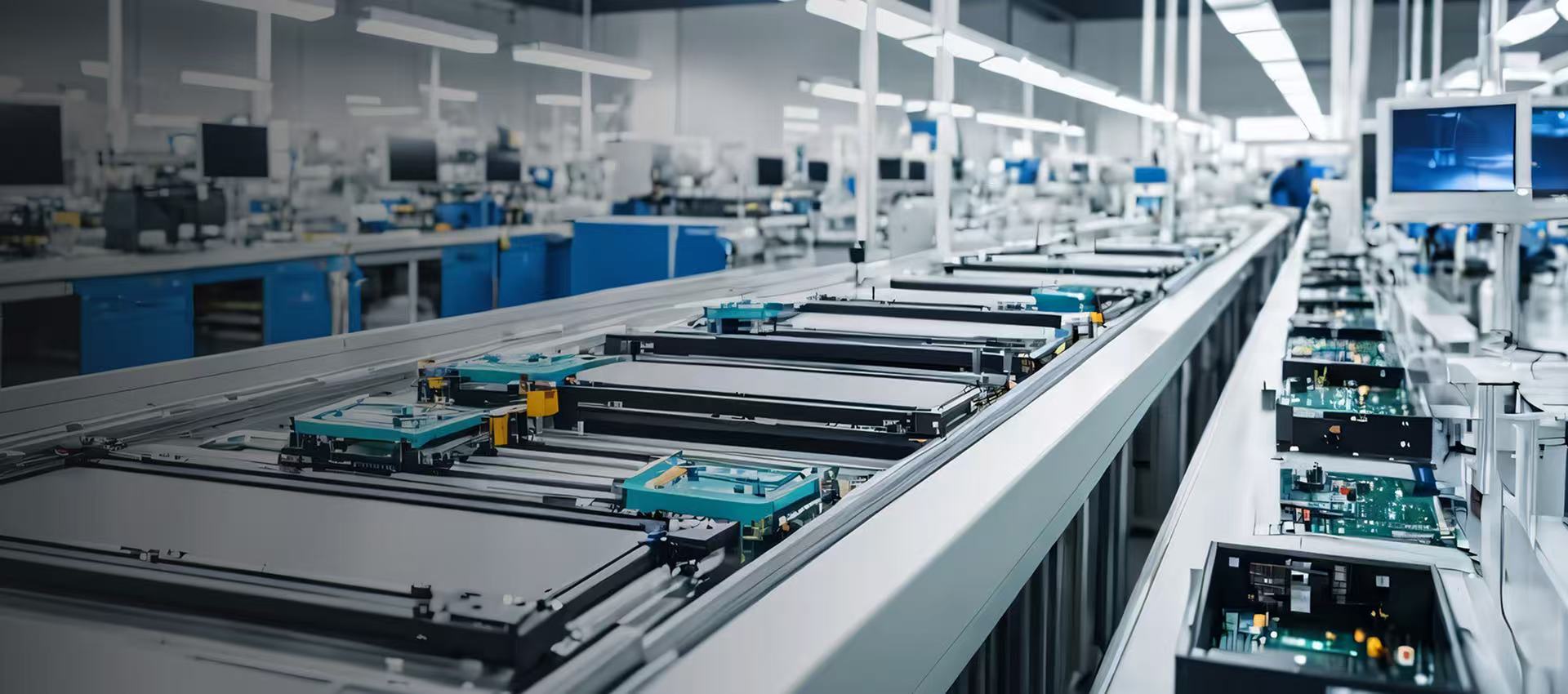
In the modern electronics industry, integrated circuit (IC) chips are like the "heart" of electronic devices, and their performance and quality are directly
related to the stability and reliability of end products. With the continuous improvement of chip integration, the internal structure is becoming
increasingly complex, and traditional detection methods often find it difficult to touch the "microscopic world" inside the chip. How to quickly and
accurately detect potential internal defects without damaging the chip has become a key challenge faced by both IC chip manufacturing and
application companies.
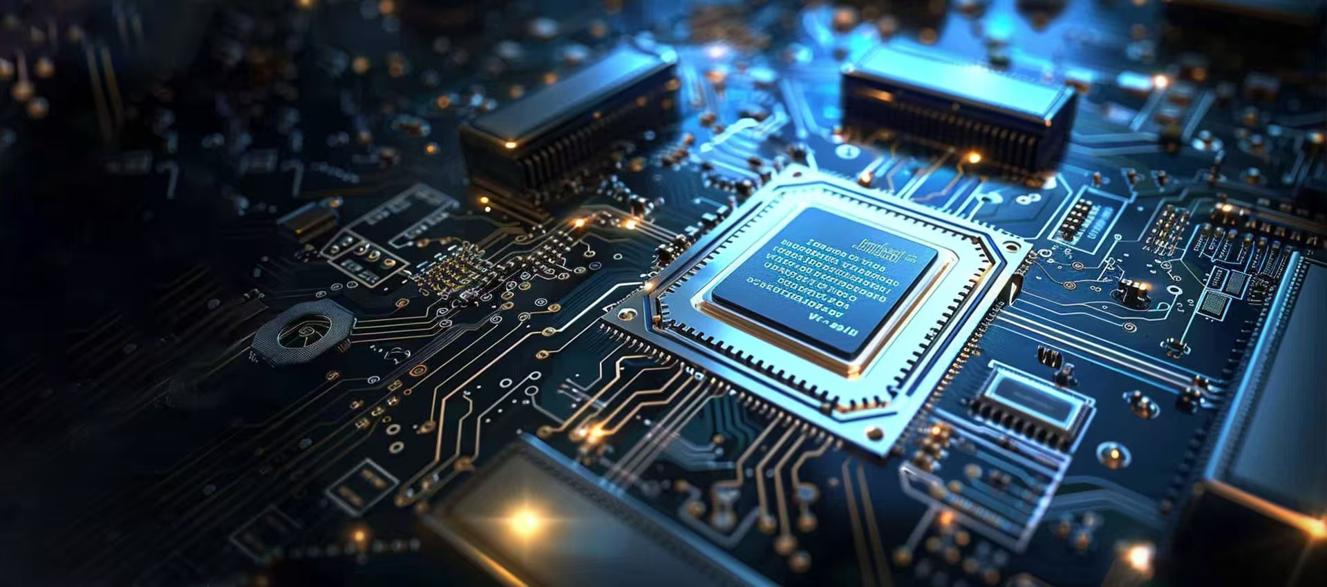
2D X-Ray Non destructive Testing Technology: The "Perspective Eye" for IC Chip Quality Assurance

2D X-ray inspection technology is a powerful non-destructive analysis tool that provides us with a pair of "perspective eyes" that can penetrate the
packaging material of IC chips, intuitively revealing their internal structure and revealing the "secrets" inside the chip without damaging the sample.
X-Ray detection technology utilizes the principle of different attenuation levels when X-rays penetrate materials to image the internal structure of IC
chips, thereby quickly and cost effectively identifying various potential defects, such as:
*Structural defects: cracks, fractures, fragments, and other structural integrity issues that directly threaten the physical reliability and long-term
stability of chips.
*Connectivity defects: Abnormal bonding wires, open circuits, short circuits, and other electrical connection issues that lead to chip functional failure
are fatal killers of product performance. As shown in the following image:

This X-ray image clearly reveals the "open circuit" defect between the lead frame and the gold wire (bonding wire) inside the IC chip. The gold wire
serves as a bridge connecting the internal circuitry of the chip with the external world. Once it breaks or has poor connections, it will directly lead to
the loss of the chip's functionality. The strength of X-Ray detection lies in its ability to accurately locate connectivity issues that are deeply embedded
without damaging the packaging, providing critical information for subsequent failure analysis and process improvement.
*Material defects: material uniformity issues such as voids, impurities, and solder residue, which affect the conductivity, heat dissipation, and long-term reliability of the chip. For example, solder residue, a seemingly small flaw that appears in an inappropriate location, can cause serious quality problems.

The above detection image shows the solder residue inside the CCD image sensor. As a precision image sensing element, any foreign object inside
the CCD (Charge Coupled Device) may affect its imaging quality and even lead to functional failure. X-Ray detection equipment can capture such
subtle internal contamination, ensuring the purity and reliability of CCD chips and even the entire IC chip.
*Size and layout anomalies: chip size deviation, die size error, internal component misalignment, etc., reflect manufacturing process deviations and
potential assembly issues.
Application scenarios of X-Ray detection: Quality control throughout the lifecycle of IC chips
X-Ray detection technology is not only applied to the final product quality inspection process, but its value runs through various stages of IC chip
design, research and development, production, and failure analysis.
*Design Verification: In the early stage of chip design, X-ray technology is used to quickly detect prototype samples, verify the rationality of the design
scheme, detect potential structural problems early, and avoid design defects from continuing into the production stage.
*Development Optimization: When introducing new packaging processes or materials, X-ray inspection can quickly evaluate the quality of process
parameters, optimize the process flow, and improve product yield and reliability.
*Production Quality Control: On the production line, X-Ray inspection equipment can sample or fully test every batch, even every IC chip, to promptly
detect and eliminate non-conforming products, prevent defective products from entering the market, and cause brand reputation and economic
losses.
*Fault Isolation: When a product malfunctions, X-ray detection can quickly locate the physical location of the failure, assist engineers in conducting
in-depth failure mechanism analysis, accelerate problem resolution, and provide a basis for subsequent improvements.
Why choose X-Ray detection?
*Non destructive testing with intact samples: The biggest advantage of X-ray testing is its non-destructive nature. The tested sample can still be used
or subjected to other analyses after testing, especially for expensive IC chips, where non-destructive testing is of great significance.
*Fast, efficient, and cost-effective: Compared to traditional destructive analysis methods, X-ray detection is faster, easier to operate, and can complete
the detection of a large number of samples in a short period of time, significantly reducing detection costs and time.
*Comprehensive perspective, insight into the interior: X-Ray can penetrate packaging materials, directly presenting the real structure inside the chip,
discovering internal defects that cannot be touched by the naked eye, and achieving a more comprehensive quality assessment.
Previous article:None